
NINGBO CHIPEX SEMICONDUCTOR CO.,LTD
Address: No. 18 Zhongheng Road, Huaxing Area, Andong Industrial Park, Hangzhou Bay New District, Ningbo
P.O.: 315300
Email: sales@chipex.cn
Tel: (86)-574-63078606;
(86)-574-63078608-8858
Semiconductor packaging technology was not valued in the past, until recently it was regarded as one of the keys to the design process, and also the key to achieving Moore's Law. According to a report on the Semiconductor Engineering website, traditionally packaging was almost never a major part of the design architecture, and the key indicators were often price and durability.
However, with the entry into sub-28nm process nodes and Internet of Things (IoT) applications, packaging is gradually becoming a market differentiation indicator, changing the past planar silicon device design and process rules. Packaging has also become a layer that must be considered in every process from initial concept to design to manufacturing.
Analysts at Tirias Research note that the traditional three pillars of semiconductor technology are lithography, transistor design, and materials. However, as it becomes increasingly difficult for lithography to achieve Moore's Law, packaging technology, which involves new materials and processing techniques, has been elevated to become the fourth major pillar.
The semiconductor industry is transitioning from 2D to 3D technology processes, and System in Package (SiP) has often become an indispensable architecture. Chip manufacturers such as Freescale, Intel, and Marvell have all successively adopted this architecture.
In some markets, design space (Form Factor) is affected by Power Budget, packaging thickness, flexibility, and other factors, making System in Package an inevitable trend. When interconnects are thicker, distances are shorter, and wiring is reduced, power consumption will also be lower.
A report by consulting firm Yole Developpement指出 that 2015 marks a new generation of electronic devices, and also the initial year for Advanced Packaging technology to enter mass production and functional roadmaps. Advanced packaging can reduce costs, improve performance, and integrate functions, and by 2020 is expected to account for 44% of all packaging services, with a market value of approximately US$30 billion.
Smartphones and tablets are the main markets for advanced packaging, while servers, PCs, gaming platforms, TVs, set-top boxes, wearable devices, and Internet of Things (IoT) applications are also expected to leverage the advantages of advanced packaging technology.
Richard Gottscho, Executive Vice President of Products at Lam Research, also noted that advanced packaging will shape a considerable market and stimulate technology markets in high-aspect ratio dielectric etch, Atomic Layer Deposition (ALD), and Through-Silicon Via (TSV) etching.
Today, the advanced packaging industry and commercial chips have adopted new packaging technologies such as fan-out, 2.5D, and monolithic 3D. However, these are not yet highly mass-produced markets, nor has a standard process experience suitable for different markets been developed. All manufacturers competing to find the best standard process are also blurring the boundaries between chips, circuit boards, and systems.
Toshiba Considers Selling Partial Stake in Chip Division
High-performance computing and networking company eSilicon is developing 2.5D chips, and eSilicon reports that demand doubled in 2015, with High Bandwidth Memory (HBM) market demand as the primary driver. Currently, the biggest challenge facing eSilicon is the interposer packaging cost and improving yield rates.
Chip packaging technology can also be handled by other companies. Many large specialized Outsourced Assembly and Test (OSAT) manufacturers are developing more advanced nanometer and packaging technologies through various means, including acquiring advanced semiconductor manufacturing equipment.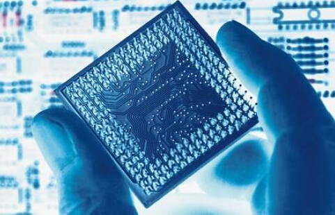
Meanwhile, major foundry giants such as TSMC, GlobalFoundries, Samsung Electronics, SMIC, and UMC are all busy upgrading advanced packaging technologies. Electronics manufacturing companies such as Foxconn and Jabil are also extending their reach beyond printed circuit boards (PCBs).
Each manufacturer adopts different technologies for different market purposes. For example, packaging technology suitable for the automotive market will be very different from that suitable for the consumer market.
The packaging method of chips can also affect other aspects of chip design. Small changes inside the packaging can significantly alter the electronic or thermal characteristics of the packaging system. There are many different assembly methods for materials inside the packaging. The application-specific ICs (ASICs), HBM, interposers, and packaging inside offer infinite combination possibilities, and there are many challenges in reuse approaches.
A major industry transformation trend is expanding from chip-level to system-level. Many manufacturers are developing new materials for various advanced packaging applications, including organic interposers, complex polymers, and more. Companies that would not previously have been associated together are now collaborating.
ASE and Japan's TDK announced in 2015 the joint establishment of ASE Embedded Electronics Incorporated, with the combined goal of producing embedded substrates and shrinking chips to 50μm thinness within a four-layer plastic substrate.
Monolithic 3D technology is expected to be the lowest-cost mass production solution. However, at that time, considerations must also be given to how many holes TSV substrates can be drilled with, the drilling speed, and the drilling density.
Processor companies such as Intel and IBM, as well as FPGA suppliers like Xilinx, will continue to pursue Moore's Law. So far, the 7nm process has been confirmed in the future roadmaps of various manufacturers, while everyone remains in a wait-and-see state regarding 5nm technology.
Process shrinkage is also becoming increasingly expensive and time-consuming. New packaging technologies serve as an alternative to improve performance, reduce power consumption, improve area efficiency, and add functions and capabilities. More and more supply chain manufacturers are beginning to provide solutions that can drive the semiconductor industry in this direction for decades to come.


