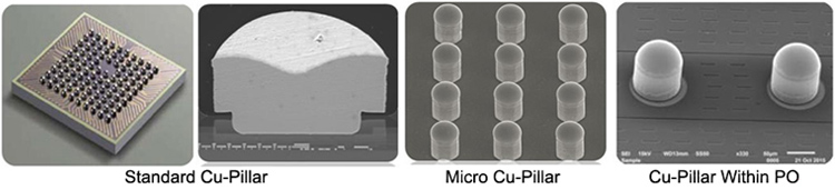
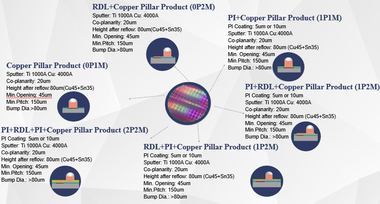
The copper bump process, also known as wafer processing, uses manufacturing techniques such as coating, yellow light, electroplating, and etching to create copper tin bumps on the surface of the chip after completing the substrate circuit. This provides "point connections" between chips and between chips and substrates, avoiding the traditional wire bonding that radiates metal "line connections" around the chip, reducing the chip area (packaging efficiency of 100%). In addition, the bump array on the chip surface can achieve high pin density, which is conducive to meeting the needs of chip performance improvement. It also has good resistance to electromigration and thermal conductivity, as well as advantages such as high density, low impedance, low parasitic capacitance, low inductance, low energy consumption, low signal-to-noise ratio, and low cost.